The Substrate as an Engineering System
The printed circuit board (PCB) — colloquially the motherboard in the context of a complete computing system — is not a passive mechanical structure for holding components in proximity. It is an active electromagnetic system whose material properties directly determine signal integrity, thermal management, manufacturing yield, and long-term reliability. The material science of PCB fabrication spans polymer chemistry, copper metallurgy, surface finish electrochemistry, and the mechanical behaviour of fibre-reinforced composites under thermal cycling.
The evolution of PCB substrate materials closely tracks the demand for higher signal frequencies and greater circuit density. The original phenolic paper boards of the 1940s and 1950s — NEMA grade FR-2 — were inexpensive but mechanically brittle, dimensionally unstable under humidity changes, and electrically lossy at high frequencies. Their replacement by woven fibreglass reinforced epoxy composites — the FR-4 family — represented a substantial advance in all measured parameters and established the material platform that dominates PCB manufacturing to the present day.
The FR-4 Composite: Structure and Properties
FR-4 designates a material grade specification rather than a single material composition. The designation (Flame Retardant grade 4) describes a woven glass fabric substrate impregnated with a brominated epoxy resin system. The glass reinforcement — typically E-glass, an alumina-borosilicate glass composition — contributes mechanical rigidity, dimensional stability under thermal excursion, and reduced thermal expansion in the plane of the board. The epoxy matrix binds the glass weave, provides electrical isolation, and determines the board's dielectric properties.
The dielectric constant (relative permittivity) of standard FR-4 is approximately 4.2 to 4.8 at 1 MHz, decreasing to roughly 3.8 to 4.2 at 1 GHz. This frequency dependence arises from the molecular relaxation dynamics of the polar epoxy resin molecules, which respond to alternating electric fields with diminishing amplitude at higher frequencies. For digital signal transmission at multi-gigabit speeds — DDR5 memory interfaces operate at effective data rates of 6400 MT/s and above — the dispersion properties of the dielectric substrate become a first-order design parameter rather than a background material property.
| Material Property | Standard FR-4 | High-Speed FR-4 | PTFE Composite |
|---|---|---|---|
| Dielectric constant (1 GHz) | 4.2 – 4.5 | 3.6 – 3.9 | 2.1 – 2.5 |
| Dissipation factor (1 GHz) | 0.020 – 0.025 | 0.008 – 0.012 | 0.0005 – 0.002 |
| Glass transition temp. (Tg) | 130–140°C | 150–175°C | — |
| Thermal conductivity | 0.25 W/m·K | 0.35 W/m·K | 0.25 W/m·K |
| CTE (x-y plane) | 14–17 ppm/°C | 13–15 ppm/°C | 12–14 ppm/°C |
Copper Foil Laminates and Signal Trace Design
The electrical conductors in a PCB are formed from copper foil laminated to the dielectric substrate under heat and pressure. Two principal copper foil types are used in high-performance applications: electrodeposited (ED) copper, produced by electroplating onto a rotating drum cathode and peeling the resulting foil free, and rolled-annealed (RA) copper, produced by rolling copper sheet to final thickness and annealing to relieve internal stress. RA copper exhibits a smooth, consistent grain structure with superior ductility under thermal cycling flexure — a significant advantage in applications subject to repeated thermal shock.
The surface roughness of the copper foil is critical for high-frequency signal integrity. At gigahertz frequencies, the skin effect confines current flow to a thin surface layer — the skin depth in copper at 1 GHz is approximately 2.1 μm. Surface roughness features with dimensions comparable to the skin depth create tortuous current paths that increase the effective conductor resistance and generate additional signal attenuation. Modern server-class PCBs specify very-low-profile (VLP) or ultra-low-profile (ULP) copper foil with Ra values below 0.5 μm to minimise this skin-effect roughness loss.
Multilayer Stack Construction
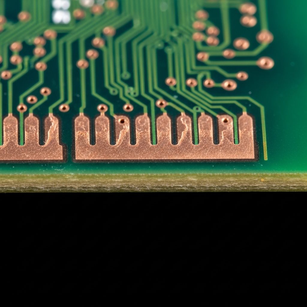
A high-complexity computing motherboard typically comprises 8 to 14 conducting copper layers separated by FR-4 prepreg dielectric layers, assembled through a sequential lamination process. The layer stack is engineered as a controlled-impedance transmission line system: signal traces on each layer are assigned characteristic impedances (typically 50 Ω single-ended or 100 Ω differential) by controlling the trace width, dielectric thickness, and relative permittivity precisely.
Vertical electrical connections between layers are formed through plated through-holes (PTH) drilled mechanically or by laser ablation. Laser-drilled micro-vias, with diameters as small as 75 μm, enable high-density interconnect in the via-in-pad constructions required by fine-pitch BGA packages. The through-hole copper plating is deposited by sequential electroless and electrolytic copper processes, with aspect ratios (depth-to-diameter ratios) of up to 10:1 achievable in production.
Surface Finish Chemistry
The exposed copper land areas of a PCB require a protective surface finish to prevent oxidation during storage and to ensure reliable solder joint formation during assembly. The choice of surface finish affects not only solderability but also the high-frequency electrical performance at the conductor-dielectric interface. Electroless Nickel Immersion Gold (ENIG) — a widely used finish consisting of a 3–5 μm electroless nickel barrier layer beneath a 0.05–0.1 μm gold surface — provides good planarity and shelf life but introduces a nickel layer with significantly higher resistivity than copper, adding attenuation on high-speed signal pads. Organic Solderability Preservative (OSP), a thin copper oxide inhibitor coating, minimises metallic surface losses but provides limited shelf life and no multiple-reflow capability.
For the highest-frequency applications — PCIe Gen 5 edge connectors, for instance — Electroless Nickel Electroless Palladium Immersion Gold (ENEPIG) finishes are specified, replacing the magnetic-permeable nickel layer with a thin palladium barrier that preserves signal integrity while maintaining adequate solderability and gold wire bondability. The material science decisions embedded in a single printed circuit board surface finish selection directly reflect the electromagnetic performance requirements at the system level.