The logic gate is the atom of computation. Every arithmetic operation, every memory address comparison, every branch prediction executed inside a modern processor reduces, ultimately, to the controlled switching behaviour of logic gates — circuits that evaluate Boolean expressions and produce binary outputs. The genealogy of this fundamental device spans nearly a century, moving from the clatter of relay contacts in telephone exchanges to the silent, near-atomic switching of complementary metal-oxide-semiconductor (CMOS) transistors etched at sub-5 nm precision into crystalline silicon.
To understand the logic gate is to understand computing itself. Its history is not merely a chronicle of miniaturisation but a record of intellectual breakthroughs, material discoveries, and engineering disciplines converging on a single goal: reliable, fast, and energy-efficient Boolean switching.
Boolean Algebra and the Conceptual Foundation
The mathematical groundwork for digital logic was laid not by an engineer but by a mathematician. George Boole, working at Queen's College Cork in the 1840s and 1850s, developed an algebraic system capable of representing logical propositions using binary values — true and false, or equivalently, 1 and 0. In his 1854 work An Investigation of the Laws of Thought, Boole demonstrated that logical deduction could be formalised as algebraic manipulation using three fundamental operations: conjunction (AND), disjunction (OR), and negation (NOT).
Boolean algebra remained a mathematical abstraction for nearly eight decades until Claude Shannon, in his landmark 1937 master's thesis at MIT, demonstrated that Boolean algebra could directly describe the behaviour of electrical relay switching circuits. Shannon's insight — that two-state electrical devices could embody two-state logical variables — provided the conceptual bridge between abstract mathematics and physical engineering. This correspondence between logic and electricity is the founding theorem of digital computing.
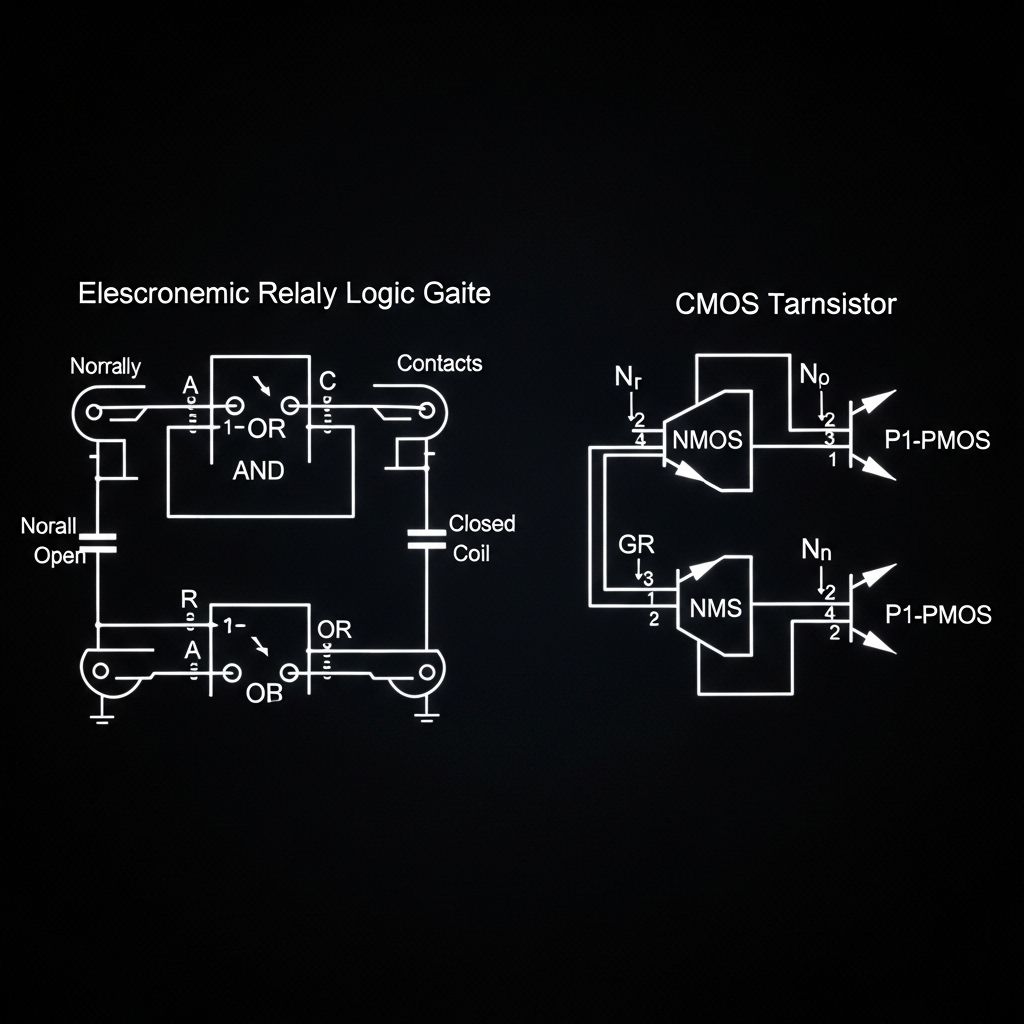
The Relay Era: Electromechanical Logic (1930s–1940s)
The earliest physical implementations of logic gates used electromechanical relays: devices in which an electromagnetic coil, when energised, deflects a spring-loaded metal contact from one electrical position to another. A relay in its de-energised state connects two terminals; when current flows through its coil, the magnetic force opens or closes the contact circuit.
AND gates could be constructed by connecting relay contacts in series — both relays must be energised for current to flow through the circuit. OR gates placed relay contacts in parallel, allowing current to flow if either contact was closed. NOT gates inverted the contact logic — a normally-closed contact produced a logical complement of its input signal.
The limitations of relay logic were severe. A relay is a mechanical device: its contact switching time is measured in milliseconds, it generates audible noise, it wears through repeated mechanical cycling, and it consumes relatively large amounts of electrical power per operation. The relay computers of the 1930s and 1940s — including Konrad Zuse's Z3 (1941) and the Bell Labs Model I (1940) — contained thousands of relay components occupying large cabinets, consuming kilowatts of power, and operating at clock frequencies measured in hundreds of hertz.
"The relay is logic made audible: the click of a contact closing is the sound of a Boolean decision being executed in steel and copper."
Thermionic Vacuum Tubes: Speed Without Mechanics (1940s–1950s)
The transition from relay to vacuum tube logic represented the first step toward purely electronic switching — circuits with no moving parts. Thermionic triodes and pentodes, originally developed for radio signal amplification, could function as switches: with no grid voltage applied, the device was non-conducting (logical 0); with a sufficient positive grid potential, plate current flowed freely (logical 1).
Vacuum tube gates switched at microsecond timescales — three to four orders of magnitude faster than relay contacts. The ENIAC (1945), often cited as the first general-purpose electronic computer, employed approximately 17,468 vacuum tubes implementing logic and memory functions across its 30 tonnes of hardware. Its clock rate reached 100 kHz for certain operations — already far beyond relay capability.
However, vacuum tubes introduced their own engineering pathologies. Each tube required a heated cathode to emit electrons thermionically, consuming substantial power and generating heat that accelerated component ageing. The mean time between failures in a machine of ENIAC's scale was measured in hours. Tube replacement became a continuous maintenance activity, and the heat generated required active cooling systems that added further to operational complexity.
The Transistor: Solid-State Switching Arrives (1947–1960s)
The invention of the point-contact transistor at Bell Laboratories in December 1947 by John Bardeen, Walter Brattain, and William Shockley opened the third and transformative chapter in logic gate history. The transistor replicated the switching behaviour of the vacuum tube in a device that required no heated cathode, operated at room temperature, consumed far less power, and occupied a fraction of the physical volume.
Bipolar junction transistors (BJTs) enabled a new family of logic gate technologies: Resistor-Transistor Logic (RTL), Diode-Transistor Logic (DTL), and Transistor-Transistor Logic (TTL). In TTL, introduced commercially in the mid-1960s by Texas Instruments, multiple-emitter transistors in the input stage replaced diode arrays, reducing propagation delay to nanoseconds and enabling reliable operation at tens of megahertz. TTL became the dominant logic family of the 1960s and early 1970s, standardised in the 7400 series integrated circuit line that remains in production today for legacy and educational applications.
| Technology | Era | Propagation Delay | Power Dissipation |
|---|---|---|---|
| Relay Logic | 1930s–1940s | ~10 ms | ~1 W/gate |
| Vacuum Tube | 1940s–1950s | ~1 µs | ~100 mW/gate |
| RTL / DTL | 1960s | ~25 ns | ~10 mW/gate |
| TTL (Standard) | 1965–1980s | ~10 ns | ~10 mW/gate |
| CMOS (4000 series) | 1970s–present | ~25–100 ns | ~0.001 mW static |
| Modern CMOS (sub-10nm) | 2010s–present | <0.1 ns | ~nW range (static) |
CMOS: The Dominant Logic Paradigm
Complementary Metal-Oxide-Semiconductor logic, first described theoretically by Frank Wanlass at Fairchild Semiconductor in 1963 and developed into practical integrated circuits through the 1970s, exploited a fundamental physical insight: p-channel and n-channel MOSFETs are electrical complements of each other. In a CMOS inverter — the simplest possible logic gate — a p-channel transistor connects the output to the supply voltage when the input is low, while an n-channel transistor connects the output to ground when the input is high. At no time are both transistors simultaneously conducting, which means the static power dissipation of a CMOS gate approaches zero. Power is consumed only during the brief switching transients when capacitances charge and discharge.
This property — near-zero static power consumption — proved decisive as transistor densities increased. TTL gates, by contrast, continuously dissipate power through their resistor networks regardless of switching activity. As integration scales increased from thousands to millions of transistors per chip, TTL's static power profile would have made dense processor construction thermally impossible. CMOS's dynamic power model, proportional to switching frequency and load capacitance, enabled progressive scaling. The relationship between CMOS power consumption and operating frequency — P = C·V²·f — became one of the central governing equations of processor design, driving the voltage scaling strategy that accompanied each successive lithographic node reduction.
From Gate to Processor: Integration and Scale
The integration of logic gates onto single silicon chips — the integrated circuit, pioneered by Jack Kilby at Texas Instruments and Robert Noyce at Fairchild in 1958–1959 — initiated the scaling trajectory that Moore's Law subsequently described. Early ICs contained tens of gates; small-scale integration (SSI) devices of the late 1960s reached hundreds; medium-scale integration (MSI) of the 1970s packaged thousands. The Intel 4004 microprocessor (1971) integrated approximately 2,300 transistors — roughly 1,150 two-transistor NAND gates — onto a 3.2 mm² die. By 2023, leading-edge processors integrated upwards of 150 billion transistors, each gate occupying an area measured in square nanometres.
The logic gate, across this journey of ninety years, has not changed in its Boolean function. An AND gate today performs exactly the operation that Shannon described in 1937, that relay engineers implemented in 1940, and that Boole formalised in 1854. What has changed is the physical substrate, the dimensional scale, and the energy cost. The relay weighing grams, operating in milliseconds, and dissipating watts has given way to a transistor of atomic dimensions, switching in picoseconds, dissipating femtojoules. The logic is immutable; the physics has been pushed to the boundary of the quantum realm.