ByteComputerRepairs Archive — Est. Milano, Italy

The Silicon
Epoch

A digital museum dedicated to the physics of semiconductors, the architecture of microprocessors, and the material heritage of computing from the relay era to the sub-nanometre gate.

Visit Virtual Exhibit
Archive Edition — March 2026
18 Scholarly Articles  ·  4 Virtual Exhibits  ·  1 Glossary
Close-up macro photograph of a 200mm silicon wafer showing iridescent circuit patterns and die grid lines under clean-room lighting Electron microscope image of individual transistor gate structures on a silicon chip, showing metallic interconnects at nanometre scale Extreme macro photograph of golden CPU socket contact pins arranged in a perfect grid on a dark motherboard surface

The Institute of Microcomputing History was founded with a singular conviction: that the engineering decisions made inside a silicon fabrication facility are as historically significant as any architectural, artistic, or industrial milestone. The transistor, first realised in germanium and later perfected in silicon, did not merely accelerate arithmetic — it restructured civilisation.

This archive curates the documented engineering record: the photolithographic processes that shrunk the gate length from micrometres to angstroms; the competing instruction set philosophies that defined two generations of processor design; the material science of boron-doped substrates and copper interconnect layers. Our approach is rigorously academic, visually cinematic, and entirely non-commercial.

We operate independently, with no affiliations to hardware manufacturers, commercial vendors, or technology service providers. Every article, exhibit, and reference entry in this archive is produced with primary-source fidelity and peer-reviewed accuracy.

The Editorial Board
ByteComputerRepairs Archive Foundation  ·  Via della Scienza 42, Milano  ·  March 2026

Three Epochs of Processor Evolution

01 1947 – 1971

The Vacuum Tube and Transistor Transition

Black and white archival photograph of early vacuum tube computer components arranged on a metal chassis with thermionic tubes visible

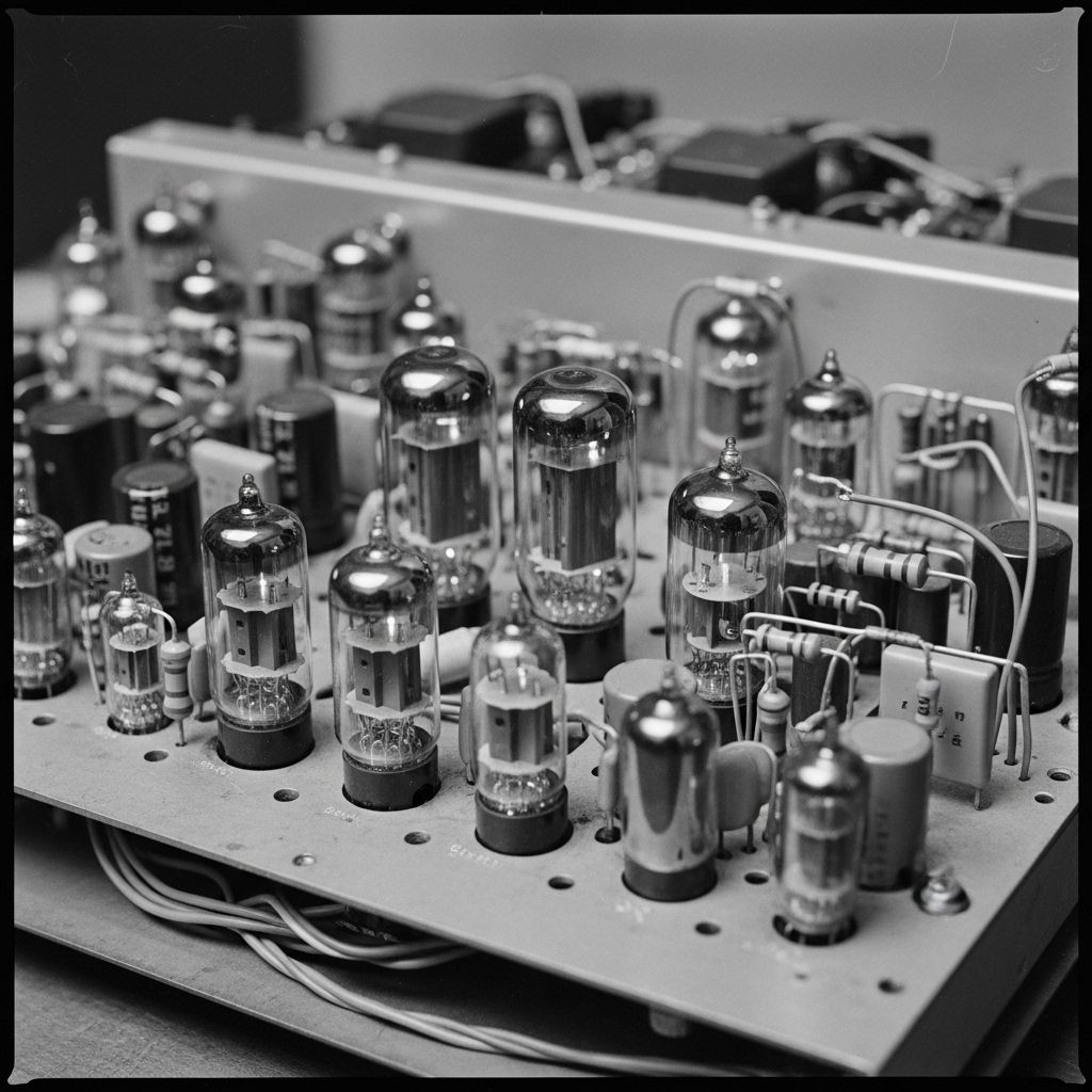
The invention of the bipolar junction transistor at Bell Labs in 1947 displaced thermionic vacuum tubes across logic circuitry. By 1960, planar transistor fabrication enabled the first commercial integrated circuits, collapsing the gap between discrete component assemblies and monolithic silicon.

Read the History
02 1971 – 2000

The Microprocessor and the RISC/CISC Debate

Macro photograph of a vintage ceramic processor package with gold lid and visible die markings from the 1980s microprocessor era

Intel's 4004 (1971) demonstrated that an entire central processing unit could occupy a single chip. The subsequent two decades saw the crystallisation of Complex Instruction Set Computing (CISC) philosophy against the challenger paradigm of Reduced Instruction Set Computing (RISC), debated in academic literature and resolved empirically through benchmark competition.

Read the Architecture Review
03 2000 – Present

The Nanometre Frontier and Quantum Effects

Colourised scanning electron microscope image of modern FinFET transistor structures showing three-dimensional fin geometry at sub-10nm scale

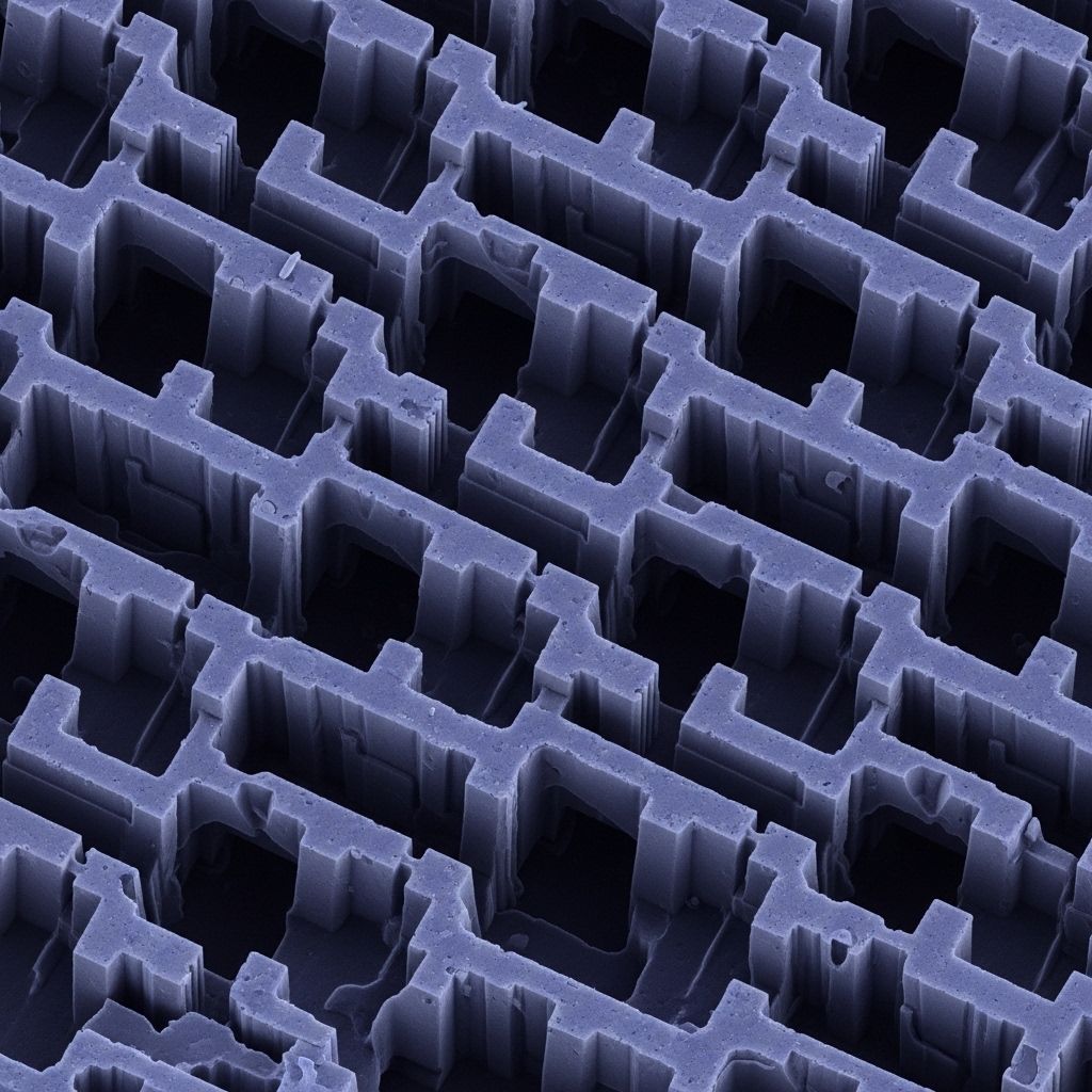
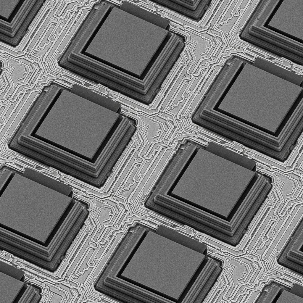
As gate lengths crossed the 10 nm threshold, quantum mechanical effects became inescapable design constraints. Tunnelling current, sub-threshold leakage, and gate-oxide breakdown demanded architectural responses: FinFET geometries, high-k dielectrics, and the exploration of alternative channel materials including silicon-germanium alloys and III-V compound semiconductors.

Explore Quantum Tunneling
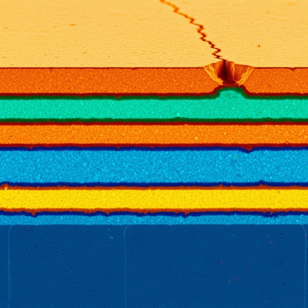
Highly magnified cross-section of semiconductor layers showing alternating silicon dioxide and polysilicon strata in vivid false-colour electron microscopy

The Semiconductor
Dictionary

From Acceptor Impurity to Zone Refining — a comprehensive alphabetical reference covering 80+ terms in semiconductor physics, photolithography, microarchitecture, and materials science. Written for engineers, historians, and informed general readers.

Access Glossary

Virtual Exhibits

Studio photograph of a 200mm polished silicon wafer with rainbow diffraction pattern on its surface, placed on a dark velvet display background

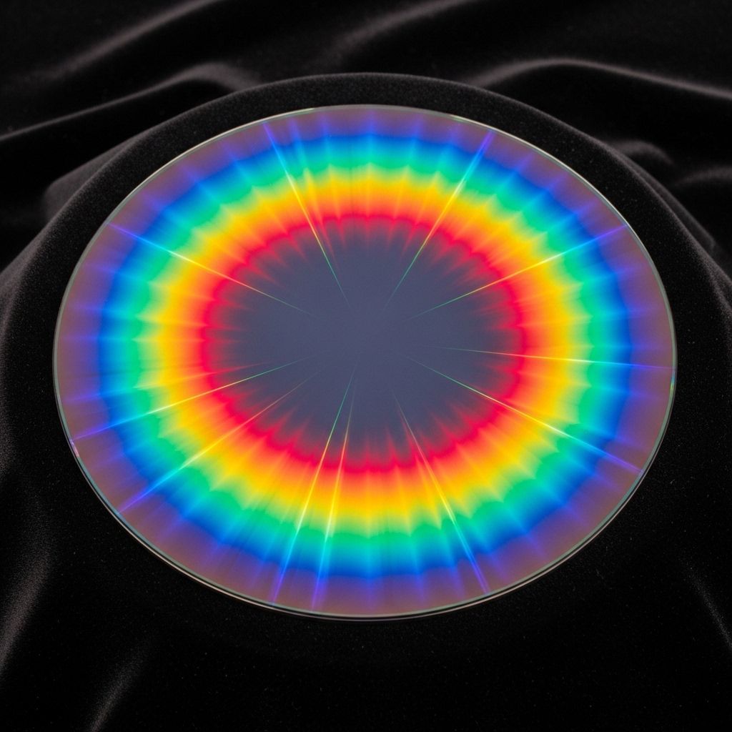
From Sand to Circuit: The Silicon Wafer Collection

Four artefacts. Four decades. The evolution of silicon substrate manufacturing from the 50mm wafers of early commercial VLSI production to the 450mm ultra-flat substrates of contemporary foundries. Each specimen is catalogued with material composition, crystallographic orientation, and manufacturing provenance.

Visit Virtual Exhibit

Frequently Asked Questions on Processor Physics

What is the physical significance of transistor gate length? +
Gate length — the distance between the source and drain of a metal-oxide-semiconductor field-effect transistor (MOSFET) — determines the fundamental switching speed and power dissipation of a logic device. Shorter gate lengths reduce the time required for charge carriers to traverse the channel, enabling higher clock frequencies. However, as gate length approaches sub-10 nm dimensions, quantum mechanical tunnelling allows electrons to pass through the gate oxide without classical barrier crossing, producing leakage current and increasing static power consumption dramatically. This physical constraint drives the transition from planar MOSFET geometries to three-dimensional structures such as FinFETs and gate-all-around nanosheets.
How does doping transform the electrical properties of silicon? +
Intrinsic silicon is a poor electrical conductor at room temperature because its valence band is fully occupied and the conduction band is largely empty. Doping introduces controlled concentrations of substitutional impurity atoms: pentavalent donors (phosphorus, arsenic) contribute free electrons to the conduction band, creating n-type material, while trivalent acceptors (boron, gallium) create holes in the valence band, forming p-type material. The interface between n-type and p-type regions — the p-n junction — constitutes the fundamental building block of diodes, bipolar transistors, and CMOS logic circuits. Doping concentrations typically range from 10¹⁵ to 10²⁰ atoms per cubic centimetre, adjusted through ion implantation and diffusion processes during wafer fabrication.
What distinguishes RISC from CISC processor architectures? +
Complex Instruction Set Computing (CISC) architectures, typified by the x86 instruction set, feature a large number of instructions with variable encoding lengths and multiple addressing modes, allowing single instructions to perform memory access and arithmetic in combination. Reduced Instruction Set Computing (RISC) architectures, developed at Berkeley and Stanford in the early 1980s, favour fixed-width instructions, load-store memory access models, and large general-purpose register files, enabling efficient pipeline implementation. The RISC philosophy reduces hardware decode complexity at the cost of increased code density, a trade-off resolved in modern implementations through micro-operation (µop) translation layers that decompose complex macro-instructions into RISC-like internal operations before execution.
Why is Moore's Law considered a historical observation rather than a physical law? +
Gordon Moore's 1965 observation that the number of transistors on an integrated circuit doubled approximately every two years was a projection derived from economic and engineering trend data, not a derivation from physical principles. Its longevity as a reliable roadmap reflected the sustained investment of the semiconductor industry in solving successive generations of lithographic, materials, and manufacturing challenges. Physical constraints — including the wavelength of extreme ultraviolet light used in photolithography, atomic-scale gate oxide thickness, and quantum effects at sub-5 nm nodes — have made continued transistor density scaling increasingly difficult and expensive. Contemporary semiconductor roadmaps acknowledge this inflection, pivoting toward three-dimensional integration, heterogeneous chiplet architectures, and novel materials as the mechanisms for continued performance scaling.

Enter the Archives

Eighteen scholarly articles, four curated virtual exhibits, and a comprehensive semiconductor glossary — assembled for engineers, historians, educators, and everyone who understands that silicon changed everything.