From Sand to Circuit:
The Silicon Wafer Collection
Four artefacts. Four decades. The evolution of silicon substrate manufacturing from the early commercial VLSI era to the ultra-flat 300mm substrates of contemporary foundries. Each specimen is catalogued with material composition, crystallographic orientation, and manufacturing provenance.
50mm Silicon Wafer — Early VLSI Era
This 50mm diameter wafer represents the substrate standard of the early commercial VLSI era. At this scale, an individual wafer could yield approximately 30–50 dies for a device geometry typical of 5–7 µm design rules. The single primary flat — ground along the (011) crystallographic plane — served as the mechanical reference for alignment fixtures in early photolithographic steppers.
The surface roughness of this specimen, measured by atomic force microscopy at the time of acquisition, records a root mean square (RMS) roughness of 0.3 nm — illustrative of the chemical-mechanical polishing (CMP) processes available in the early 1970s, adequate for multi-micron lithography but insufficient for sub-100 nm device fabrication. The specimen is housed in a nitrogen-purged archival container to prevent native oxide growth from altering its surface state.
The transition from 50mm to 75mm wafers, standardised in the mid-1970s, increased usable die area per wafer by approximately 125%, directly reducing per-die fabrication cost at constant yield and providing the economic driver for the next generation of manufacturing infrastructure investment.
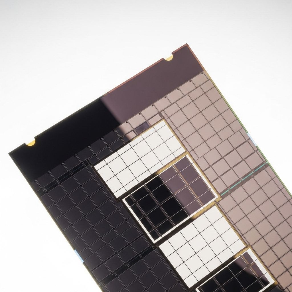
100mm Processed Wafer — CMOS Transition Period
This partially processed 100mm wafer, bearing several completed photolithographic layers in a 3 µm CMOS process, documents the pivotal transition in semiconductor manufacturing when CMOS began displacing NMOS and bipolar logic as the dominant technology family for microprocessor and memory fabrication.
The visible die grid pattern — each die measuring approximately 8 × 6 mm — represents a logic device of the era: roughly 50,000 to 200,000 transistors per die. The secondary flat at 90° to the primary flat identifies this as a p-type <100>-oriented wafer by the SEMI M1 wafer flat convention in use before the adoption of laser-scribed notches for 200mm and above substrates.
The thermal budget of the 3 µm process represented in this specimen — comprising multiple furnace oxidation, diffusion, and anneal cycles at 900–1100°C — would be incompatible with advanced sub-100 nm processes, where minimising thermal exposure is critical to preventing dopant redistribution and degradation of shallow junction profiles.
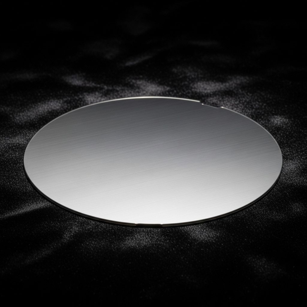
200mm Silicon Wafer — Deep Sub-Micron Era
This 200mm diameter prime-grade polished wafer, sourced from an archived batch produced during the transition from 180 nm to 130 nm CMOS node manufacturing, exemplifies the substrate quality required for deep sub-micron semiconductor fabrication. The notch visible at the wafer edge replaced the dual-flat system of earlier generations, enabling more precise rotational alignment in automated wafer-handling equipment and maximising the usable area of the wafer edge.
The iridescent interference pattern visible across the polished surface results from the native silicon dioxide layer (approximately 1.5–2 nm thick) formed by atmospheric oxidation after the final polishing step. This thin-film interference, analogous to the colours of a soap bubble, illustrates the extreme surface quality achieved: surface roughness below 0.15 nm RMS is mandatory for gate oxide formation at 130 nm and below, as surface roughness directly contributes to carrier mobility degradation through scattering at the Si/SiO₂ interface.
The controlled interstitial oxygen content — specified to ASTM F121 — serves a dual purpose: dissolved oxygen provides mechanical strengthening of the wafer (preventing warpage during high-temperature processing) while also acting as a precipitation precursor for intrinsic gettering zones that capture metallic contaminants away from the active device region.
300mm Silicon Wafer — Advanced Node Substrate
This 300mm epitaxial prime-grade wafer represents the current production substrate standard for advanced logic and memory fabrication at technology nodes from 10 nm down to 3 nm and below. The epitaxial silicon layer — a thin, highly controlled crystalline film grown by chemical vapour deposition on the polished substrate — provides a defect-free starting material for transistor formation, free from the oxygen precipitate nuclei present in the Czochralski-grown bulk material beneath.
The site flatness specification — SFQR (Site Flatness Quality Range) below 30 nm across each 26×8 mm exposure site — is dictated by the depth of focus of extreme ultraviolet (EUV) lithography scanners. With a depth of focus measured in tens of nanometres, any wafer surface variation exceeding this tolerance will cause lithographic defocus, producing pattern distortion that propagates directly into yield loss. Meeting this specification requires three-stage chemical-mechanical polishing, in-situ topography measurement, and feedback-controlled polishing corrections at the sub-nanometre scale.
The transition from 200mm to 300mm wafer manufacturing, completed across the industry between 1999 and 2005, increased usable wafer area by 225% relative to 200mm substrates, providing a fundamental cost reduction per transistor at constant process technology. The transition required complete replacement of wafer-handling robotics, deposition chambers, lithography stages, and inspection tools — representing cumulative capital investment of hundreds of billions of dollars across the global semiconductor manufacturing industry.
Deepen Your Understanding
The journal articles and semiconductor glossary provide the theoretical context behind the artefacts in this virtual exhibit collection.